Imagine trying to hear a single pin drop in the middle of a loud rock concert. That captures the challenge of recording faint biomagnetic fields from the human brain against ambient magnetic noise. In high-precision quantum magnetometry, any stray magnetic source nearby distorts delicate measurements. Detecting femtotesla-scale neural signals or minuscule geophysical shifts requires optoelectronic hardware that introduces zero magnetic pollution into the sensor head.
For decades, optoelectronics manufacturing has relied on Kovar for hermetic packaging. While well-suited for standard optical transceivers, this nickel-iron-cobalt alloy is inherently ferromagnetic. Positioned near a zero-field atomic vapor cell, standard packaging materials compromise measurement sensitivity.
To overcome these constraints, the quantum sensing sector is transitioning toward custom, non-ferromagnetic chip-scale components. Achieving optimal signal-to-noise performance requires replacing standard alloy packaging with non-magnetic alternatives engineered specifically for spin-exchange relaxation-free physics.
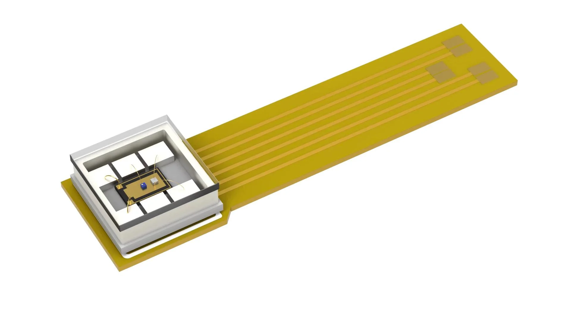
The Vanishing Field: Why Quantum Sensors Require Magnetic Silence
The human brain generates electrical currents across billions of active neurons, producing magnetic fields that rarely exceed 10 to 100 femtoteslas at the scalp. Earth’s geomagnetic field, by comparison, measures roughly 50 microteslas—nearly nine orders of magnitude stronger.
| Parameter | Earth's Geomagnetic Field | Typical Human Alpha Rhythm (MEG) | Evoked Sensory Responses |
|---|---|---|---|
| Typical Magnitude | ~50 µT (5 × 10⁻⁵ T) | ~1–2 pT (10−12 T) | ~10–100 fT (10−14–10−13 T) |
| Relative Scale | Baseline reference | 25–50 million times smaller | 500 million–5 billion times smaller |
| Packaging Sensitivity | Tolerates standard metals | Susceptible to ferromagnetic drift | Requires very low-remanence components |
While magnetically shielded rooms suppress external ambient noise, they cannot shield a sensor cell from its own internal housing. When the optical source sits millimeters from an alkali vapor cell, local residual magnetism limits the device's baseline resolution.
How a SERF Magnetometer Operates at the Absolute Edge of Detection
Spin-exchange relaxation-free magnetometers operate by heating an alkali vapor (rubidium, cesium, or potassium) within an isolated glass cell. Under normal conditions, rapid collisions between gas atoms randomize atomic spins, causing decoherence.
When the ambient magnetic field drops near zero (< 10 nT) and atomic density is sufficiently high, the spin-exchange rate outpaces the atomic Larmor precession frequency. In this regime, spin-exchange collisions no longer destroy macroscopic polarization. The atomic ensemble behaves coherently, enabling a SERF magnetometer to achieve sensitivity levels below 1 fT/√Hz, matching or exceeding liquid-helium-cooled superconducting quantum interference devices (SQUIDs).
← Near-Zero Magnetic Field (<10 nT)
Residual magnetism from nearby packaging can induce Larmor precession and compromise SERF magnetometer operation.
The Mechanism of Field-Induced Decoherence
Maintaining spin exchange relaxation-free conditions requires strict suppression of residual bias fields. Stray magnetic moments create localized field gradients across the vapor cell. Rather than experiencing uniform zero-field conditions, atoms in different regions precess at varying frequencies. This broadens optical resonance lines, destabilizes baseline calibration, and drops the instrument out of the SERF regime.
The Kovar Dilemma in High-Sensitivity Instruments
Standard TO-can and butterfly optoelectronic housings rely heavily on Kovar (ASTM F15: ~54% Fe, 29% Ni, 17% Co). Engineers originally adopted this formulation because its coefficient of thermal expansion closely matches borosilicate glass, ensuring dependable glass-to-metal hermetic seals across broad operating temperature ranges.
However, each constituent element in Kovar is ferromagnetic.
Residual Magnetism and Sensor Instability
Ferromagnetic components display magnetic hysteresis: once exposed to a magnetic field, they retain a remanent magnetization (Br). Even when degaussed before assembly, Kovar components can pick up stray magnetization from assembly tools, environmental fields, or operating drive currents.
Thermal cycling and physical movement can alter the effective residual magnetic field. In a multichannel sensor array, moving a sensor head containing residual ferromagnetic mass introduces dynamic offsets that obscure authentic neural or geophysical signals.
Packaging Gradients in Optically Pumped Magnetometer Laser Diode Units
Directly integrating an optically pumped magnetometer laser diode inside the sensor housing reduces size and eliminates coupling losses from optical fiber bundles. Yet standard optical packaging can introduce multiple magnetic elements:
- Header Base and Cap: Spun or stamped Kovar alloys.
- Lead Pins: Iron-nickel alloy cores.
- Diffusion Barriers: Electrolytic or electroless nickel flash (1–5 µm) applied under final gold plating to prevent copper-gold interdiffusion.
- Internal Thermistors & Submounts: Nickel-bearing metallization layers.
These layers can create steep spatial magnetic gradients. In the dipole approximation, magnetic field strength decreases with the inverse cube of distance (B ∝ 1/r3). Placing standard nickel-plated headers just 5–10 mm from an alkali cell can introduce substantial field distortions, depending on the residual magnetization and component geometry. Such disturbances may exceed the tolerable limits for SERF operation.
Engineering the Architecture of a Non-Magnetic VCSEL
Overcoming this limitation requires rebuilding the optoelectronic package from non-ferromagnetic materials. Vertical-Cavity Surface-Emitting Lasers (VCSELs) serve as compact optical sources for miniaturized atomic sensors. Their low operating currents, near-circular output beams, and vertical emission allow compact optical layouts without complex anamorphic correction optics.
A genuinely non-magnetic VCSEL requires avoiding ferromagnetic materials across every sub-assembly: the submount, packaging headers, feedthrough pins, window caps, and internal bonding solders.
| Packaging Component | Standard Industry Material | Ultra-Low Remanence Replacement | Technical Advantage |
|---|---|---|---|
| Package Header / Base | Kovar (Fe-Ni-Co alloy) | Pure Titanium / High-Purity Aluminum Oxide (Al2O3) | Low magnetic susceptibility; suitable thermal and mechanical properties depending on package geometry |
| Diffusion Barrier | Electroplated Nickel (1–3 µm) | Platinum (Pt) or Titanium-Tungsten (TiW) | Avoids ferromagnetic nickel underlayers; solder compatibility depends on the metallization stack |
| Feedthrough Lead Pins | Kovar / Alloy 52 | Phosphor Bronze / High-Purity OFHC Copper | Low magnetic remanence and improved electrical and thermal conductivity |
| Cap & Optical Window | Kovar cap with glass seal | Titanium or Ceramic cap with sapphire window | Potential for hermetic sealing and high optical transmission at alkali pump wavelengths |
| Die Attach & Interconnects | Nickel-bearing braze / leadframes | Eutectic Gold-Tin (AuSn 80/20) / Pure Gold wire bonds | Avoids ferromagnetic joining materials; offers reliable electrical and mechanical connections with suitable processing |
Eliminating Nickel Flashing
Standard commercial manufacturing relies on nickel as an intermediate barrier to limit diffusion between gold finishes, solder, and underlying copper traces. In ultra-low remanence packaging, the nickel layer is completely omitted. Refractory metallization layers, including sputter-deposited titanium-tungsten (TiW) or platinum (Pt), can provide diffusion resistance while avoiding the ferromagnetic behavior associated with nickel.
Hermetic Sealing Without Parasitic Dipoles
Alkali-based quantum magnetometers require optical sources with high operational reliability. Uncooled semiconductor laser junctions can degrade if exposed to atmospheric oxygen or ambient humidity over extended deployments.
Non-magnetic packaging can achieve hermetic protection through active metal brazing and flux-free gold-tin eutectic soldering. Optical windows made from anti-reflective coated sapphire or optical-grade quartz are metallized along their perimeter using non-magnetic thin films, then joined to ceramic or titanium headers.
Hermeticity can be evaluated using applicable MIL-STD-883 helium leak procedures. Depending on package geometry and qualification requirements, a helium leak-rate target below 1 × 10⁻⁹ atm·cm3/s may be specified. Actual performance must be verified on the finished package.
Advancing Neuroimaging: The MEG Optical Sensor
The most immediate medical application for non-magnetic laser diodes is magnetoencephalography (MEG). MEG captures real-time brain dynamics by recording weak cortical magnetic fields generated during neuronal activity.
Historically, clinical MEG systems required arrays of low-temperature superconducting quantum interference devices (SQUIDs), cooled using liquid helium within bulky cryogenic dewars. Conventional systems position sensors within a rigid helmet, restricting head movement during measurements.
- Liquid Helium Dewars
- Rigid, Heavy Helmet
- Fixed Subject Posture
- High Infrastructure Cost
- Room-Temperature Operation
- Flexible Scalp Cap
- Greater Motion Freedom
- Closer Sensor-to-Scalp Placement
Integrating an optoelectronic MEG optical sensor allows magnetometer arrays to operate without cryogenic cooling. This removes the need for liquid helium systems and creates opportunities for lightweight, patient-conforming sensor caps.
Wearable Systems and VCSELs for MEG
Modern neuroimaging arrays use modular, 3D-printed sensor caps that position optically pumped magnetometers close to the scalp. Because magnetic fields weaken rapidly with distance, reducing the separation between the sensor and the brain can improve signal detection.
In the magnetic dipole approximation, field magnitude decreases approximately as B ∝ 1/r3. Conventional SQUID systems place sensors behind cryogenic insulation, while wearable OPM systems can achieve substantially smaller scalp-to-sensor clearances.
Cryogenic SQUID-MEG
Wearable OPM-MEG
Building dense, multichannel helmets requires individual sensor modules to be lightweight, power-efficient, and thermally controlled. A dedicated VCSEL for magnetoencephalography (MEG) systems can provide a compact optical pump with milliwatt-level optical output.
VCSELs offer compact emission geometry and efficient electrical operation. Sensor designers must still account for drive electronics, vapor-cell heating, and thermal isolation to maintain safe and comfortable operating conditions near the scalp.
Clinical Utility of Motion-Tolerant Brain Mapping
Magnetically clean, compact optical packages can help extend brain imaging into applications where conventional fixed-position systems are difficult to use.
- Pediatric Care: Conformal sensor caps can accommodate different head sizes and allow greater freedom of movement. This may make brain monitoring easier for children who struggle to remain still.
- Epilepsy Monitoring: Wearable OPM systems can support studies involving motor tasks, speech exercises, and selected movement conditions while recording neural activity.
- Functional Neuroscience: Researchers can examine cortical activity during more natural behavioral tasks, including controlled movement and physical interaction. Motion compensation and magnetic field control remain essential.
Semiatom GmbH: Custom Non-Magnetic Packaging for SERF Sensor Heads
Every quantum sensing platform has specific optical, mechanical, and magnetic requirements. Standard commercial laser packages may not provide the wavelength accuracy, polarization characteristics, or magnetic cleanliness required near sensitive atomic vapor cells.
Semiatom GmbH develops VCSEL solutions for quantum sensing, magnetometers, and precision photonics. Its portfolio includes non-magnetic VCSEL packaging and customized configurations intended to reduce unwanted magnetic influence around sensitive sensor assemblies.
Optical Precision and Package Tailoring
Semiatom GmbH works with customers to select optoelectronic configurations suited to their atomic sensing requirements. Important parameters include:
- Targeted Alkali Wavelengths: VCSEL selection around the rubidium D1 transition at 795 nm and cesium D1 transition at approximately 895 nm. Other wavelengths, including potassium-related requirements, require project-specific evaluation.
- Polarization Control: Evaluation of polarization stability, operating current, temperature dependence, and external optical components needed to obtain the required polarization state.
- Ultra-Low Remanence Housings: Non-magnetic package options using carefully selected structural materials, metallization, electrical connections, and optical interfaces to reduce magnetic disturbance.
- Integrated Micro-Optics: Application-specific optical windows and beam-conditioning components can be evaluated according to the available space and optical requirements.
Combining wavelength selection, optical characterization, and appropriate packaging materials helps developers integrate VCSELs into compact atomic sensor systems while controlling unwanted magnetic and thermal effects.
The Path Forward in Quantum Precision
Quantum sensing is moving beyond laboratory demonstrations toward compact instruments suitable for practical deployment. The atomic physics behind spin-exchange relaxation-free magnetometry is well established, but successful system integration depends on magnetic cleanliness, optical stability, temperature control, and packaging quality.
Replacing ferromagnetic package materials with carefully selected low-remanence alternatives helps reduce local magnetic interference. These improvements are particularly relevant when optical sources must be positioned close to sensitive vapor cells.
Whether used in wearable MEG systems or compact magnetometers for geophysical sensing, non-magnetic optoelectronic packaging can contribute to cleaner measurements and more stable sensor operation.
Frequently Asked Questions
Why does Kovar degrade the performance of atomic magnetometers?
Kovar is an iron-nickel-cobalt alloy with ferromagnetic properties and magnetic remanence. When positioned near an atomic vapor cell, Kovar components can generate stray fields and magnetic gradients that disturb the low-field conditions required for sensitive atomic magnetometry.
What materials are used to replace Kovar in ultra-low remanence laser packaging?
Possible alternatives include high-purity aluminum oxide ceramics (Al2O3), titanium, oxygen-free copper, and phosphor bronze. Nickel-containing metallization can be replaced with selected platinum or titanium-tungsten (TiW) barrier layers, subject to soldering and reliability requirements.
What advantages do VCSELs offer over edge-emitting DFB lasers in wearable quantum sensors?
VCSELs provide a compact emitting structure, near-circular beam geometry, and efficient low-power operation. These characteristics can simplify optical alignment and help reduce sensor-head dimensions. Actual power consumption, linewidth, beam divergence, and polarization stability depend on the selected device and operating conditions.
Can non-magnetic packaging maintain hermetic reliability over long service lifetimes?
Yes, properly engineered ceramic or titanium packages can provide hermetic protection using compatible sealing and soldering techniques. Hermeticity must be verified on the completed assembly using applicable procedures such as those in MIL-STD-883. Long-term reliability depends on the specific material interfaces, process control, and environmental qualification.
Which custom parameters can Semiatom GmbH adjust for atomic sensor development?
Semiatom GmbH offers VCSEL selection and package customization for precision photonics applications. Customers can discuss wavelength, optical output, package dimensions, material restrictions, optical windows, and non-magnetic packaging requirements. Available configurations depend on the selected device and project specifications.
Explore Semiatom high-power VCSEL solutions or non-magnetic VCSEL packaging options for additional technical information.